DCDarknet 11 Badge Instructions for DEFCON 30

Posted on April 08, 2022

Introduction

This year's Darknet (11) is a Printed Circuit Cardboard (PCCB), which will let us focus more on teaching basic electronics rather than soldering. In past years, most people followed the instructions on how to assemble the badge, but spent very little time learning how or why the badge works.

By using a paper badge and supplying you with the parts, we're giving you the freedom and the know-how to design your own circuit, your own custom badge.

Please note this is not an exhaustive electronics course, this is enough information to get you started and playing around, so some things have been greatly simplified and or glossed over.

Badge Levels

Definitions

Parts

BOM (Bill of Materials)

Formulas

Badge Level 1

Badge level 1 consists of a power supply (batteries and battery pack) (BT1), resistors (R#), and LEDs (D#).
LEDs have a maximum current that can go through them, if we exceed that current, then a LED will pop like a balloon with too much air. We must limit the amount of current that an LED receives. To limit the current, we use resistors. The LEDs that we are using have a rating of ~0.02 amps.
We can use Ohm's Law to calculate what the resistance needs to be for the LEDs. We know that the power being supplied will be 4.5 V (3 AAA batteries in series (1.5 * 3)), and we know that the current should be ~0.02 amps.
There is one more critical piece that we need to learn about LEDs: LEDs have something called forward voltage. LEDs need to have current to turn on, but they also consume voltage as it passes through them. In our case, all LEDs have a forward voltage of 2.1 V, which is also the minimum voltage that is required to turn on the LED.
So if we just had a single LED in this circuit, the math is easy.

V = IR
4.5 - 2.1 = 0.02 * R
2.4 = 0.02 * R
2.4 / 0.02 = R
120 = R

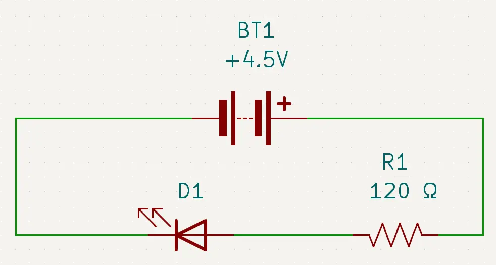
So in this example, we would need 120 Ω of resistance for that LED. So we would put ~120 Ω resistor in the circuit between the power supply and the LED.

A screenshot of a circuit diagram that has the positive of a 4.5V battery (BT1) connecting in serial to a 120 Ω resistor (R1) that connects to the anode of an LED (D1) whose cathode then connects back to the negative of the 4.5V battery (BT1).

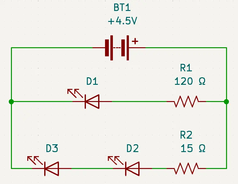
But wait, our circuit is a little more complex than that. We have 3 LEDs in total. Two of the LEDs are wired in series (D2, D3) and 2 LEDs are wired in parallel (D1, D2). One of the parallel lines only has 1 LED (D1).
Since we know that LEDs in parallel (D1, D2) will receive the same voltage, than we know the single LED (D1) will use the formula that we used above.

V = IR
4.5 - 2.1 = 0.02 * R
2.4 = 0.02 * R
2.4 / 0.02 = R
120 = R

So the single LED (D1) will still use the 120 Ω resistor (R1).
But the other line contains 2 LEDs wired in series (D2, D3). Remember the definition of a series circuit, all parts receive the same current, but the voltage will drop. So 2 LEDs in series (D2, D3) will still need ~0.02 amps, but will consume twice the amount of voltage. So our formula for the 2 LEDs in series (D2, D3) will look like this:

V = IR
4.5 - (2 * 2.1) = 0.02 * R
4.5 - 4.2 = 0.02 * R
0.3 = 0.02 * R
0.3 / 0.02 = R
15 = R

So for our 2 LEDs wired in series (D2, D3) we will need to have ~15 Ω resistor (R2).
To sum everything up, for our level 1 badge, we will need to have a power supply, 3 LEDs, and at least 2 resistors. The single LED (D1) will need to have a ~120 Ω resistor (R1), and the 2 LEDs (D2, D3) will need to have a ~15 Ω resistor (R2).

A screenshot of a circuit diagram that has the positive of a 4.5V battery (BT1) connecting in serial to a 120 Ω resistor (R1) that connects to the anode of an LED (D1) whose cathode then connects back to the negative of the 4.5V battery (BT1). The postive of the 4.5V battery (BT1) also has a parallel connection to a 15 Ω resistor (R2) that connects in serial to the anode of an LED (D2) whose cathode connects to the anode of another LED (D3) whose cathode connects back to the negative of the 4.5V battery (BT1).

Badge Level 2

Badge level 2 consists of a power supply (batteries and battery pack) (BT1), resistors (R#), capacitors (C#), transistors (Q#A), and LEDs (D#) to make a blinking badge.
Oooooo
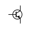
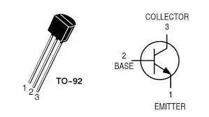
The transistor will act as a switch between its collector and emitter depending on the voltage of the base. The goal will be to supply voltage to the base. When the voltage of the base hits ~0.7V the switch will close and power will flow between the emitter and the collector.
When the voltage is below ~0.7V the switch is open which prevents power from flowing:

A screenshot of the electronics symbol for an open switch

When the voltage is above ~0.7V the switch is closed, which allows power to flow:

A screenshot of the electronics symbol for a closed switch

Now that we have a base understanding of transistors, lets start to design our circuit.
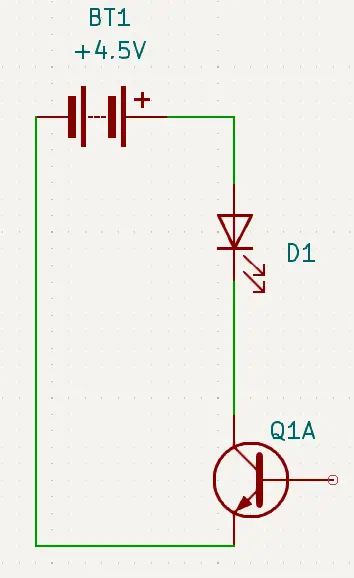
We know that for an LED to work, it has to have power flow the anode to the cathode. So in our circuit design, we will need to have power (red) (BT1) flow into the anode of the LED (D1), the connect the cathode of the LED (D1) to the collector of the transistor (Q1A), and then have the emitter of the transistor (Q1A) connect back to the negative (blck) (BT1) of the power supply.

A screenshot of a circuit diagram that has the postive of a 4.5V battery (BT1) connecting in serial to the anode of a LED (D1) whose cathode connects to the collector of a transistor (Q1A) whose emitter connects back to the negative of the 4.5V battery (BT1).

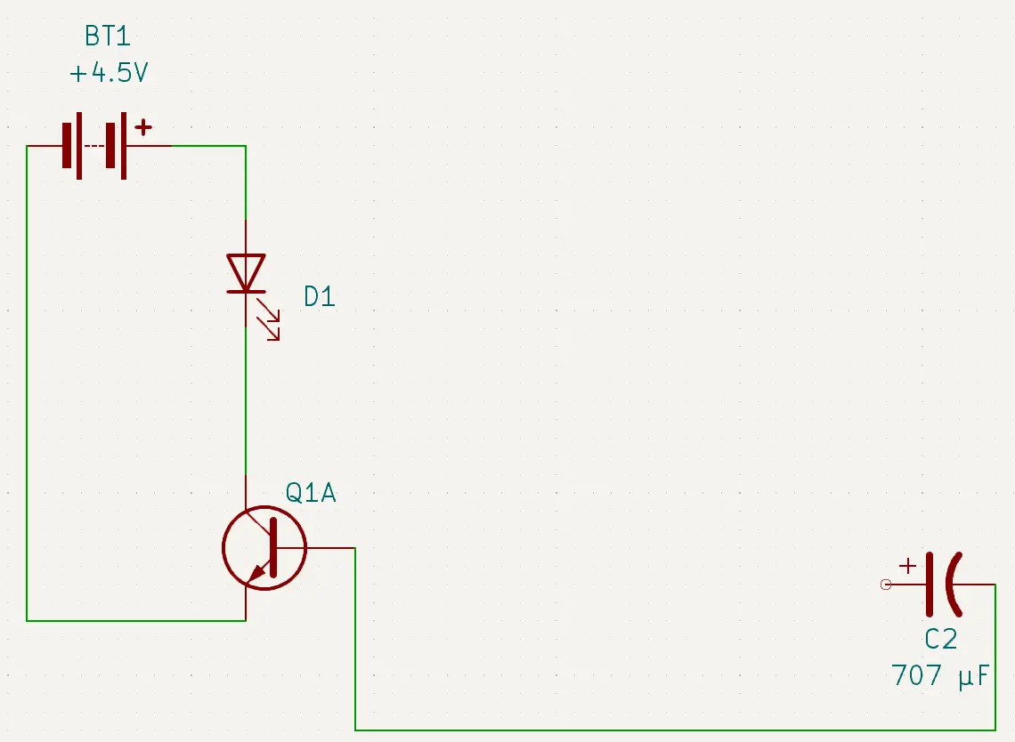
Hmmm, but now we need to connect something to the base of the transistor (Q1A) that will supply ~0.7V sometimes, but not all of the time. Out of the components that we have, do we have something that will first charge itself, and then discharge itself? Why yes, yes we do. We have capacitors. Remember, a capacitor will allow power to flow from positive to negative while it charges, and when it is fully charged it will then discharge itself in the opposite direction. So lets add a capacitor (C2) to our circuit:

A screenshot of a circuit diagram that has the postive of a 4.5V battery (BT1) connecting in serial to the anode of a LED (D1) whose cathode connects to the collector of a transistor (Q1A) whose emitter connects back to the negative of the 4.5V battery (BT1). The base of the transitor (Q1A) connects to the negative of a capacitor (C2).

Now we haver a new problem, where do we connect the positive side of the capacitor (C2) to? We need to connect it to some place that it can receive a charge so that it can discharge into the base of our transistor (Q1A). What if we double our circuit and add another LED (D2), transistor (Q2A), and capacitor (C1)? By doing this, we can create what is called a bistable multivibrator circuit. As one capacitor is charging the other capacitor is discharging. This will cause us to have one LED on, and one LED off, and then the circuit will flip, and the LED that was off will now be on, and the LED that was on will now be off.

A screenshot of a circuit diagram that has the positive of a 4.5V battery (BT1) that connects in parallel to the negative of a capacitor (C1), the base of a transitor (Q2A), the anode of a LED (D1), the anode of a LED (D2), the negative of capacitor (C2), and the base of transitor (Q1A). The positive of capacitor (C1) and the cathode of LED (D1) connects to the collector of (Q1A). The positive of capacitor (C2) and the cathode of LED (D2) connects to the collector of (Q2A). The emitter of both transistors (Q1A, Q2A) connect to the negative of the 4.5V battery (BT1).

Looking at this circuit, we can see that we have the negatives of the capacitors (C1, C2) attached to the bases of the transistors (Q1A, Q2A) and that we have the positive of the capacitors (C1, C2) attached to the collectors of the opposite transistors (Q1A, Q2A). So when LED (D1) is on, it will be charging the capacitor (C1). When capacitor (C1) is full, it will discharge ~0.7V into the base of the transistor (Q2A) causing the switch to close between the emitter and the collector of transistor (Q2A). This will then turn on LED (D2) which will light up and start to charge the capacitor (C2). When capacitor (C2) is charged, then the cirucit will flip back to LED (D1) lighting up, and capacitor (C1) charging while capacitor (C2) discharges, and LED (D2) is off.
There is one problem with our circuit though, we need to add in resistors to protect the components by limiting the amount of current each component receives.
We have two LEDs (D1, D2) in parallel, so we can use Ohm's Law to calculate the resistance that we need to protect the LEDs. Refer to Badge Level 1 for how to use Ohm's Law.
But we also need to add resistors to the capacitors (C1, C2). This is where we can use the RC Time Constant formula defined in the formulas section.
As an example, let's use 707 μF capacitors and 1357 Ω resistors. To calculate the blinking frequency we would:

f = 1/(τRC)
f = 1 / (6.28 * R * C)
f = 1 / (6.28 * 1357 * 0.00707)
f = 1 / (8521.96 * 0.00707)
f = 1 / 60.2502572
f = 0.016597439521 Hz

So in this case, the LEDS (D1, D2) would blink at a rate of ~0.0166 times per second, or once every 6 seconds.
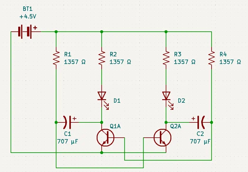
This means that we will be adding 2 resistors (R2, R3) to protect each of the LEDs that are wired in parallel, and adding 2 resistors (R1, R4) for the capacitors to determine the blinking frequency.
Our final circuit will look something like this:

A screenshot of a circuit diagram that has the positive of a 4.5V battery (BT1) that connects in parallel to a 1357 Ω resistor (R1) that connects to the negative of a capacitor (C1), the base of a transitor (Q2A). A 1357 Ω resistor (R2) to the anode of a LED (D1). A 1357 Ω resistor to the anode of a LED (D2). A 1357 Ω resistor to the negative of capacitor (C2), and the base of transitor (Q1A). The positive of capacitor (C1) and the cathode of LED (D1) connects to the collector of (Q1A). The positive of capacitor (C2) and the cathode of LED (D2) connects to the collector of (Q2A). The emitter of both transistors (Q1A, Q2A) connect to the negative of the 4.5V battery (BT1).

Badge Level 3

Badge level 3 consists of a power supply (batteries and a battery pack) (BT1), resistors (R#), capacitor (C1), 555 Timer IC (U1), and a LED (D1).
Instead of transistors like we used in badge level 2 we will be using the 555 Timer IC (U1) in what is called an astable mode. Astable means that the 555 Timer IC (U1) will oscillate or fluctuate between off and on. This oscillation will be what causes the LED to blink.
The oscillation that we will be using is called a square wave:
A screenshot of a square wave
When working with square waves, we need to look at a couple of time measurements. The first is how long is the square wave at its peak, and the second is how long is teh square wave at its valley.
The square wave peak will determine how long the LED is on for, and the square wave valley will determine how long the LED is off for. Basically it will tell us what the blinking rate of the LED is.
We will start off with an example using the 555 Timer IC (U1) formula that we defined in the formula's section.
As an example let's use a 8412 ohm resistor (R1), a 369 ohm resistor (R2), and a 707 μF capacitor (C1). To calculate the square wave and therefore the blink rate, we will start with the Time High:
Thigh = 0.7 * (R1 + R2) * C1
Thigh = 0.7 * (8412 + 369) * 0.00707
Thigh = 0.7 * 8781 * 0.00707
Thigh = 6146.7 * 0.00707
Thigh = 43.457169

Then to calculate the square wave Time Low we would:
Tlow = 0.7 * R2 * C1
Tlow = 0.7 * 369 * 0.00707
Tlow = 258.3 * 0.00707
Tlow = 1.826181

So in this example the LED (D1) will turn on for ~ 43 seconds, and then it will turn off for ~2 seconds. Basically the LED (D1) will stay on for a long time and then it will blink off quickly and turn back on.

Now that we know how to calculate what the blink rate is using a square wave, we can start to design our circuit using the 555 Timer IC (U1). But first we need to learn a little about the 555 Timer IC (U1).
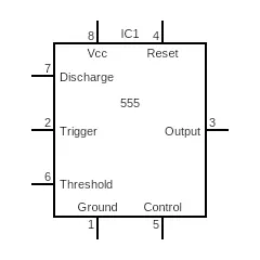
The 555 Timer IC (U1) has a total of 8 pins:
  1. Ground (GND)
    The ground pin (1) is used as ground for power to flow towards. As we apply voltage it will flow towards the ground pin.
  2. Trigger (TR)
    The trigger pin (2) is used to determine when the output pin needs to be turned on. This is triggered (hehehe) by reaching a threshold of less than 1/3 of the supplied voltage.
  3. Output (Q)
    The output pin (3) is where the power goes if the trigger pin is activated. So the output pin is either low, which means that it isn't supplying voltage (or very low voltage), or it is high, which means that it is outputting close to the voltage supplied.
  4. Reset (R)
    The reset pin (4) is like the old reset button on your Nintendo (yes I am that old). When pressed it will reset the state of the IC until the trigger is triggered. To activate the reset pin, we attach it to the ground.
  5. Control (CV)
    The control pin (5) is used to try and level out fluctuations in the voltage supplied. Usually this is just connected to the ground or the negative on the power supply.
  6. Threshold (THR)
    The threshold pin (6) is used to determine when the output pin needs to be turned off. This is triggered by reaching a threshold (hehehe) of more than 2/3 of the supplied voltage.
  7. Discharge (DIS)
    The discharge pin (7) will act as a ground or negative to discharge whatever is in the IC while it is on.
  8. Vcc (VCC)
    The Vcc pin (8) is connected to the positive end of the power supply. The power supply needs to supply a minimum of 4.5 volts.
So now that we know a little bit about how the 555 Timer IC (U1) works, we can really start to design our circuit.
We know that we need to have power (red) go to Vcc (Pin 8), but we also want power (BT1) to go to Reset (Pin 4) as well. The reason that we are supplying power to Reset is that we don't want Reset to go to the ground and reset our IC (U1).
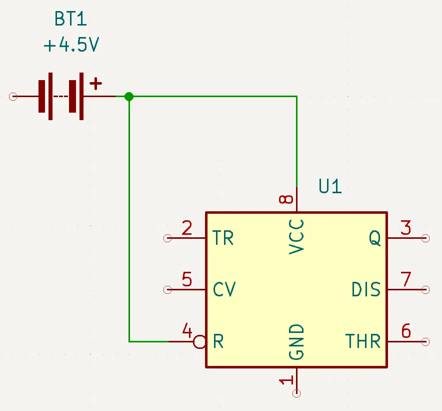
A screenshot of a circuit diagram that has the positive of a 4.5V battery (BT1) that connects in parallel to a 555 timer IC (U1) on pin 8 (VCC) and pin 4 (R).

We also know that we need to have Ground (Pin 1) connect to negative (black) (BT1).
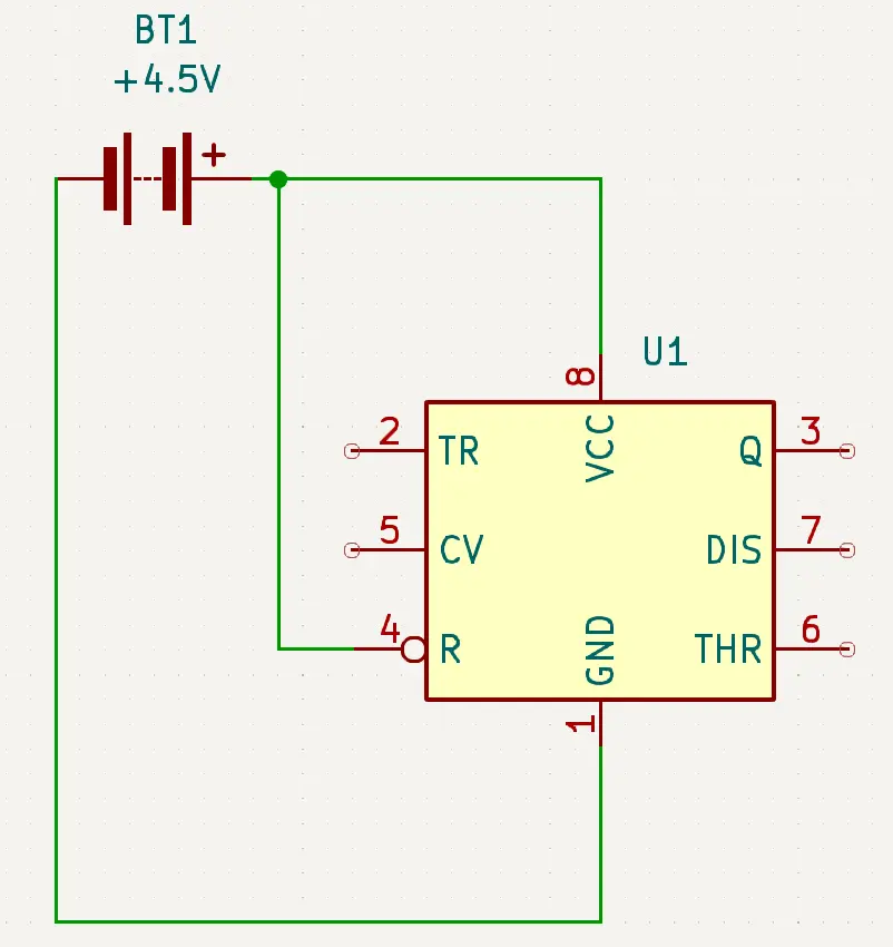
A screenshot of a circuit diagram that has the positive of a 4.5V battery (BT1) that connects in parallel to a 555 timer IC (U1) on pin 8 (VCC) and pin 4 (R). The 555 timer IC (U1) pin 1 (GND) connects to negative of the 4.5V battery (BT1).

We know that Output is where the power will output itself, so that is where we need to connect the anode of the LED (D1). But remember, a LED needs a resistor inline so that it doesn't pop. So please use Ohm's Law to determine the resistor (R3) value to place before the anode. We will also need to connect the cathode of the LED (D1) to the negative (black) (BT1).
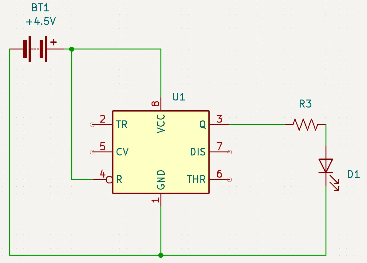
A screenshot of a circuit diagram that has the positive of a 4.5V battery (BT1) that connects in parallel to a 555 timer IC (U1) on pin 8 (VCC) and pin 4 (R). The 555 timer IC (U1) pin 3 (Q) connects to a resistor (R3) which connects to the annode of a LED (D1) whose cathode connects to the 555 timer IC (U1) pin 1 (GND) which connects to negative of the 4.5V battery (BT1).

This is where the circuit gets a little bit tricky, as we need to connect the Discharge (Pin 7), the Threshold (Pin 6), and the Trigger (Pin 2). We will also need to add in a couple of resistors (R1, R2) and a capacitor (C1).
We know that when the IC (U1) is off, meaning that the Threshold (Pin 6) has more than 2/3 voltage, that the Discharge (Pin 7) is on. We will use the Discharge (Pin 7) to charge the capacitor (C1).
So to begin with, we need to connect the Discharge (Pin 7) to a resistor (R1). We also need to make sure that we have a complete circuit so we will attach the resistor (R1) to power (red).
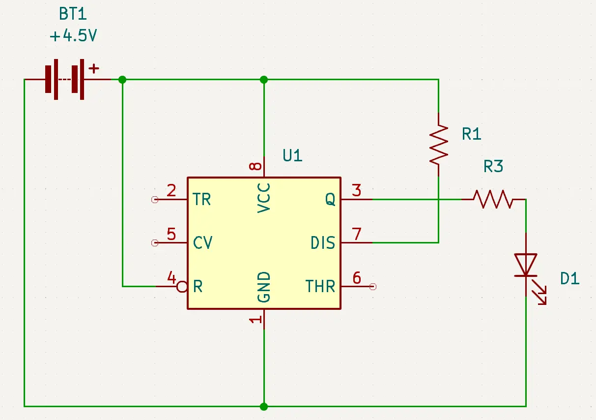
A screenshot of a circuit diagram that has the positive of a 4.5V battery (BT1) that connects in parallel to a 555 timer IC (U1) on pin 8 (VCC), pin 4 (R), and a resistor (R1) that connects to the 555 timer IC (U1) pin 7 (DIS). The 555 timer IC (U1) pin 3 (Q) connects to a resistor (R3) which connects to the annode of a LED (D1) whose cathode connects to the 555 timer IC (U1) pin 1 (GND) which connects to negative of the 4.5V battery (BT1).

Since the Discharge (Pin 7) will be used to charge the capacitor (C1), we need to add a resistor (R2) between Discharge (Pin 7) and the capacitor (C1). This resistor (R2) will slow the charge of the capacitor (C1) and therefore determine the vallue (low) of the square wave (how long the LED is off for).
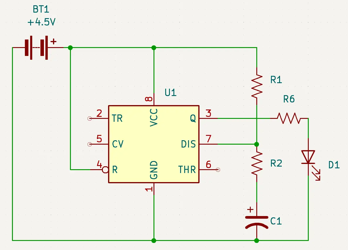
A screenshot of a circuit diagram that has the positive of a 4.5V battery (BT1) that connects in parallel to a 555 timer IC (U1) on pin 8 (VCC), pin 4 (R), and a resistor (R1) that connects to the 555 timer IC (U1) pin 7 (DIS) and a resistor (R2) which connects to the positive of a capacitor (C1). The 555 timer IC (U1) pin 3 (Q) connects to a resistor (R3) which connects to the annode of a LED (D1) whose cathode connects to the 555 timer IC (U1) pin 1 (GND) and the negative of a capacitor (C1) which connects to negative of the 4.5V battery (BT1).

Lets go a little more in depth into this. So when we turn on the power supply (BT1), the capacitor (C1) will be discharged, meaning it is like a dead battery. Also since we just applied power, we know that the Trigger (Pin 2) will be at less than 1/3 supplied voltage, so the IC (U1) will turn on and the LED (D1) will turn on. The Discharge (Pin 7) will also turn on, and begin to charge the capacitor (C1) through the resistors (R1, R2). Once the capacitor (C1) goes over the 2/3 supplied voltage required for the Threshold (Pin 6) then the IC (U1) will turn off, turning off the LED (D1) and Discharge (Pin 7) of the IC (U1). The IC (U1) will stay off until the capacitor (C1) is disharged. Once the capacitor (C1) goes below the 1/3 supplied voltage for the Trigger (Pin 2) then the IC (U1) will turn on, which will turn on the LED (D1) and the Discharge (Pin 7). This process will continue to repeate itself turning the LED (D1) on and off based on the values of the capacitor (C1) and the resistors (R1, R2).
So now, we just need to connect the Trigger (Pin 2) and the Threshold (Pin 6) to the capacitor (C1) and our circuit should be complete.
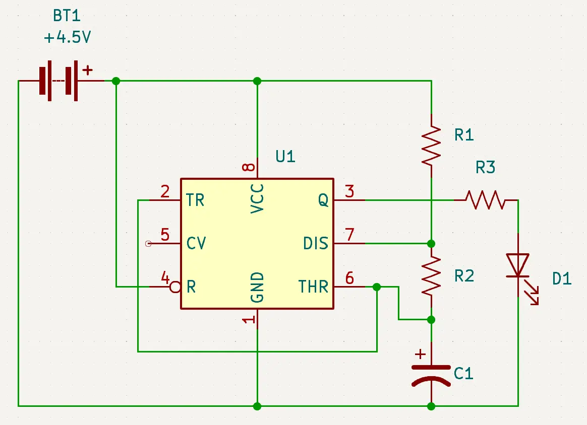
A screenshot of a circuit diagram that has the positive of a 4.5V battery (BT1) that connects in parallel to a 555 timer IC (U1) on pin 8 (VCC), pin 4 (R), and a resistor (R1) that connects to the 555 timer IC (U1) pin 7 (DIS) and a resistor (R2) which connects to the 555 timer IC (U1) pin 6 (THR) which connects to both the 555 timer IC (U1) pin 2 (TR) and the positive of a capacitor (C1). The 555 timer IC (U1) pin 3 (Q) connects to a resistor (R3) which connects to the annode of a LED (D1) whose cathode connects to the 555 timer IC (U1) pin 1 (GND) and the negative of a capacitor (C1) which connects to negative of the 4.5V battery (BT1).

Since we have such a complicated circuit, lets recap how it works:
When the Trigger (Pin 2) is less than 1/3 supplied voltage, then the IC (U1) will pass power through the Output (Pin 3) which will power the LED (D1) turning the LED (D1) on. It will also pass power through the Discharge (Pin 7).
The Discharge (Pin 7) is connected to the capacitor (C1) through a series of resistors (R1, R2), so when the IC (U1) is on, it will start to charge the capacitor (C1). Once the capacitor (C1) reaches 2/3 of supplied voltage, then it will activate the Threshold (Pin 6). When Threshold (Pin 6) is activated, then the IC (U1) will turn off, and the LED (D1) will turn off. While the IC (U1) is off, the Discharge (Pin 7) will also be off.
When the capacitor (C1) drops below 1/3 supplied voltage, then the Trigger (Pin 2) will activate and turn the IC (U1) back on.
This process will repeat itself for as long as there is power supplied to the circuit, causing the LED (D1) to blink according to the values calculated for the square wave.

Congratulations, you, in theory have a working Darknet 11 level 3 badge.

Darknet 11 Black Badge

If you made it this far, and you completed all 3 levels, then please find Gulo so that he may give you the Darknet 11 black badge.
While supplies last